ACSM Industrial Thin Layer Graphene Nanoplatelets
Product Detail
ACS Material Industrial Thin Layer Graphene Nanoplatelets are a production-scale family of few-layer graphene platelets supplied in three grades — Type A, B, and C — each tuned for a different balance of thickness, lateral size, and electrical conductivity. All three are black/grey powders with >99% carbon, produced for conductive and mechanical reinforcement in batteries, composites, coatings, and electronics at industrial volumes.
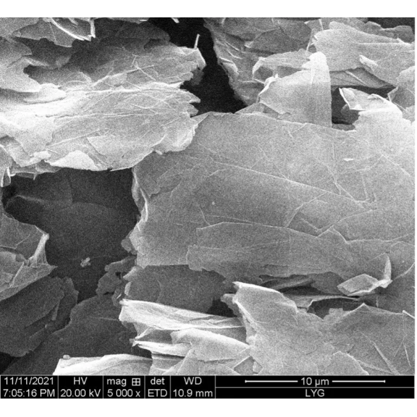
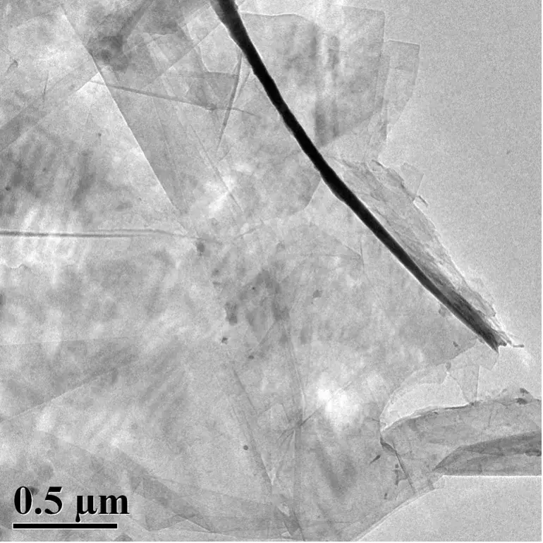
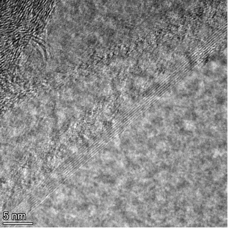
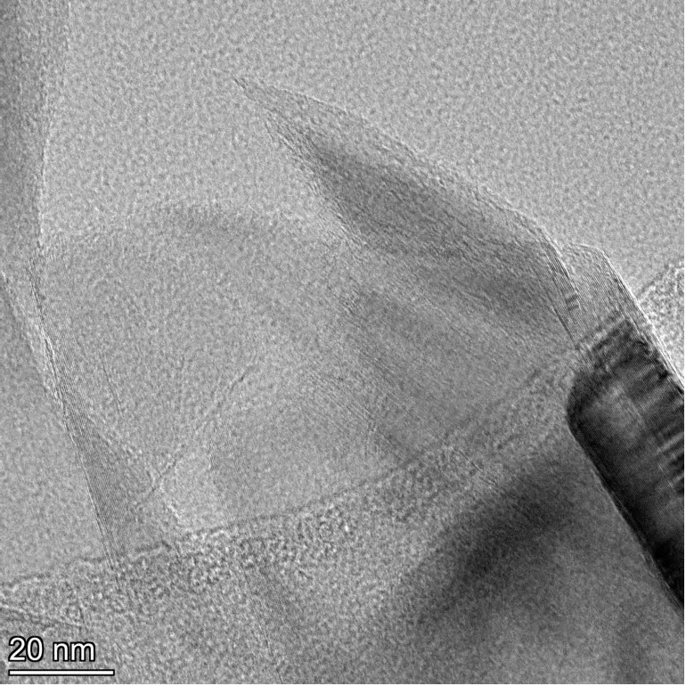
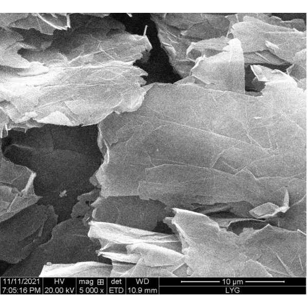
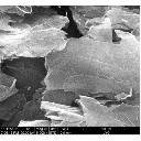
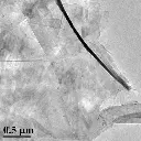
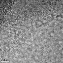
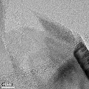
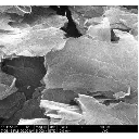
Thin-layer graphene nanoplatelets are stacks of just a few graphene sheets — thin enough to expose a large fraction of their carbon at the surface, yet far more robust and economical than single-layer graphene. Across the three grades, thickness runs from about 1 to 6 nm and lateral platelet size from roughly 1 to 10 µm, letting you match aspect ratio, conductivity, and packing density to your process. Industrial quantities are available; contact ACS Material for pricing and lead time.
Specifications
| Parameter | Type A | Type B | Type C |
|---|---|---|---|
| Appearance | Black/grey powder | Black/grey powder | Black/grey powder |
| Diameter (lateral size) | 1–5 µm | 1–6 µm | 1–10 µm |
| Thickness | 1–6 nm | 1–4 nm | 2–3 nm |
| Tap density | 0.06–0.1 g/mL | 0.05–0.07 g/mL | 0.04–0.06 g/mL |
| Apparent density | 0.04–0.07 g/mL | 0.03–0.05 g/mL | 0.03–0.05 g/mL |
| Electrical conductivity | 800–1100 S/cm | 800–1100 S/cm | 800–1100 S/cm |
| Carbon content | >99% | >99% | >99% |
| Water content | <2 wt% | <2 wt% | <2 wt% |
| Residual impurities | <1 wt% | <1 wt% | <1 wt% |
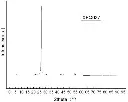
| Particle-size distribution (D50) | ~26.03 µm | ~16.01 µm | ~9 µm |
| Specific surface area (BET) | ~29.8 m²/g | — | — |
| Preparation method | Physical liquid-phase exfoliation | — | — |
The particle-size distribution (D50) is measured by laser diffraction on the dry powder and reflects loosely held agglomerates of platelets, not the size of an individual sheet (the lateral size of a single platelet is given by the Diameter row). Agglomerates can partially break down during compounding and dispersion, depending on shear, formulation, and surface treatment. SSA and preparation method are characterized for Type A; Type B and C belong to the same industrial thin-layer family. Values are typical and may vary lot to lot — consult the TDS for the specification of a given lot.
Application fields
- New-energy batteries — conductive additive for electrodes
- Antistatic & conductive composites and coating modifiers
- Thermal management — heat dissipation, thermally conductive composites
- Mechanical reinforcement — improved strength and stiffness
- Electronics & basic research — graphene transistors, electronic chips, antenna materials
- Aerospace and other lightweight high-performance materials
Choice of grade depends on the target property: all three grades offer high conductivity (800–1100 S/cm); Type C has the largest lateral size and lowest D50 for network formation, while the grades differ mainly in thickness, lateral size, and powder density. Graphene nanoplatelets are typically dispersed into the host matrix with a coupling agent; the optimal loading and modifier depend on your formulation.